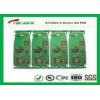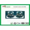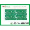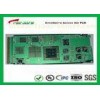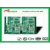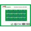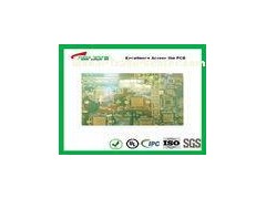


14 Layer GPS PCB FR370 Quick Turn PCB Prototypes BGA and IC pad size 350x200mm
TECHNOLOGY:
. RoHS/ Lead Free
. HDI Microvias
. Blind Vias
. Buried Vias
. Selective Plating
. Impedance Control
Manufacturing Standard:
. IPC-A-600G Class II
. IPC-A-600G Class III
. PERFAG 2E for Double-Sided Board
. PERFAG 3C for Multilayer Board
Capability
Min. Finished Holes Size: 0.008" (0.20mm)
Micro vias diameter: 0.004 TO 0.010 inches (0.10 - 0.25mm)
Minimum line width/spacing: 0.004/0.004 inches (0.10mm/ 0.10mm)
Maximum copper thickness: 5oz (140um)
Thin board thickness:
. DS - 0.008 inches (0.20mm)
. 4/L - 0.016 (0.40mm)
. 6/L - 0.020 inches (0.60mm)
Maximum board thickness:
. 275.8mil (7.0mm)
Surface treatment:
. HASL/lead free HAL/gold plating
. Immersion gold
. Immersion tin
. Immersion silver
. Gold fingers (hard gold)
. OSP
14 Layer GPS PCB FR370 Quick Turn PCB Prototypes BGA and IC pad size 350x200mm